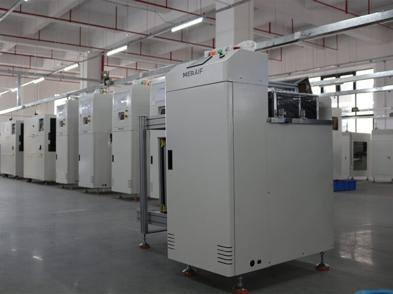
Most SMT vendors love a neat spec line. Minimum package here, maximum body size there, maybe a flashy CPH number for decoration. But when I look at whether a line can really run a broad mix, I don’t start with the brochure—I start with the defects nobody wants to talk about once production gets messy.
Because that’s the thing. A machine can physically place a tiny chip and still lose the job at the printer, the oven, the support pins, the nozzle library, or AOI tuning. Same with large components. Same with “mixed capability” claims. It looks fine. Usually.
Why Component Size Range Is More Than a Placement Spec
I frankly believe this is where buyers get misled first.
A published SMT component size range sounds precise, almost courtroom-clean, but it hides the ugly part of the conversation: what happens after the head drops the part, the board flexes a touch, paste volume varies a little lot-to-lot, and the thermal mass of one ugly power connector starts bullying the rest of the assembly during reflow. That is the actual test.
And yet, people still shop as if placement range equals process capability. It doesn’t. Not even close.
For very small packages, the line usually gets exposed at the print stage—aperture design, paste release, pad geometry, component stability, all the fussy stuff that production managers hate because it doesn’t fit nicely on a sales slide. For larger or heavier parts, the center of gravity shifts: board support, nozzle fit, transport stability, keep-out spacing, soak behavior, wetting consistency. Different headache. Same invoice.
That’s why I’d rather hear a supplier talk about mixed SMT lines or turnkey SMT line solutions in terms of yield windows and changeover control than “full-range flexibility.” That phrase means almost nothing until somebody shows process data.
What 0201 Components Actually Mean in Production
Here’s an old industry sin that keeps wasting time: people say “0201” as if there’s zero ambiguity.
There is.
In imperial naming, 0201 usually means about 0.6 mm x 0.3 mm. In metric naming, though, some suppliers use 0201M or 008004 for something far smaller—around 0.25 mm x 0.125 mm. That’s not a tiny paperwork issue. That changes land pattern assumptions, stencil decisions, inspection thresholds, rework feasibility, and even whether the team in the room is discussing the same part at all.
From my experience, this is where projects start drifting before anyone notices. One engineer says 0201. The sourcing team hears 0201. The line builder nods. But they’re not necessarily picturing the same package, and by the time someone catches it, the stencil file and the process plan are already moving in the wrong direction.
A good 2024 example shows why that matters. The 2024 SMTA case study on 0201 BTC diode assembly tracked assembly work using a DEK NeoHorizon printer, Parmi SigmaX SPI, and ERSA Hotflow 10 reflow setup, and the interesting bit wasn’t just that tiny parts are hard—everybody knows that—it was that the aperture design with the better transfer efficiency didn’t automatically deliver the cleaner assembly result. That’s a very factory-floor kind of finding. Annoying. Useful. Real.
So when people ask how to assemble 0201 components, my answer is never “buy a more accurate placer.” That’s too clean. Too easy. It’s a print-place-reflow-inspect stack, and if one layer is sloppy, the whole thing starts coughing defects.
Where Smallest SMD Components Usually Fail
But let’s be honest about where the line usually cracks.
Not at the headline spec.
The smallest packages tend to punish weak stencil design, inconsistent paste release, bad board support, lazy placement tuning, and overconfident AOI logic. A lot of teams still treat smallest SMD components as a placement challenge, when they’re really a process discipline audit with sharp teeth. If the line is drifting, these parts will rat you out fast.
And this is where jargon starts to separate real operators from brochure writers. I want to hear about area ratio, aperture wall quality, gasketing behavior, support-pin strategy, solder balling risk, false-call rates, SPI thresholds, and how AOI is being tuned so it’s not just screaming at harmless variation all shift long. That’s factory language. That’s useful language.
A credible solution also doesn’t pretend one box solves everything. It has to link the pick-and-place machines, the solder paste printer, the reflow ovens, and the inspection strategy into one stable loop. Otherwise, you’re not buying capability. You’re buying arguments between departments.
Why Oversized PCB Parts Create a Different Set of Risks
Now flip the board over mentally and look at the other end of the range.
Big parts misbehave differently.
Oversized components don’t usually embarrass a line because the gantry can’t reach them. They embarrass it because mass, height, odd geometry, or thermal demand starts breaking the comfortable assumptions built around standard SMT flow. Connectors, transformers, shielding cans, bulky power modules, tall electrolytics—they all show up with their own version of trouble, and none of that trouble cares how pretty the placement speed chart looked during the sales meeting.
Here’s the ugly truth: a lot of “wide-range” lines are only wide-range until the heavy or awkward parts arrive. Then manual assists creep in. Offline handling appears. Support tooling gets improvised. Profiles get bent around the big package and smaller joints start paying the price.
That’s why best PCB assembly for oversized parts is the wrong question if it’s aimed only at machine size compatibility. The better question is whether the full process can hold together when one section of the board suddenly needs more support, more thermal control, and more mechanical discipline than the rest. If the answer is vague, I assume the risk is real.
And the market pressure behind this isn’t hypothetical. In November 2024, NIST announced funding of up to $300 million for advanced packaging research, with expected total investment above $470 million—a pretty blunt signal that package complexity and integration density are rising, not easing off. Meanwhile, Reuters reported in March 2024 that AI-driven demand for advanced packaging had pushed TSMC to consider more capacity expansion, including more CoWoS output. Read the advanced packaging funding announcement and Reuters’ report on advanced packaging demand. The signal is pretty clear: assemblies are getting denser, stranger, hotter, and less forgiving.
How to Evaluate 0201 to Oversized Component Handling
So what should a buyer actually do?
Start asking better questions.
Not “What is your minimum package?” That’s brochure talk. Ask how stencil design is validated for ultra-small passives. Ask how board support is configured when tall or heavy bodies sit near fine-pitch areas. Ask what happens to thermal profiling when one side of the board carries parts with very different heat demands. Ask how many false AOI calls the team tolerates before they retune the algorithm instead of blaming operators.
That’s where reality lives.
And the timing matters. The Semiconductor Industry Association reported that global semiconductor sales in 2024 exceeded $600 billion, up 19.1% year over year. When demand rises like that, factories try to squeeze broader product mixes through the same footprint, the same crews, and sometimes the same imperfect process assumptions. That’s when 0201 to oversized component handling turns from a technical footnote into a margin problem. The SIA’s 2024 market update is worth a look because it frames the commercial pressure behind all this process stretching.
Personally, I trust suppliers who can point to customer cases and explain their process quality controls in plain manufacturing terms. Even better if they can show how they separate needs between prototype small-batch lines and high-speed mass production lines. That usually means they’ve already learned the expensive lessons.
A Practical Comparison of Small and Oversized Part Demands
| Component category | Typical issue | Primary process concern | What a capable line should demonstrate |
|---|---|---|---|
| 0201 components | Skew, bridging, insufficient or excessive paste | Stencil design, SPI control, placement stability | Repeatable print transfer, tight AOI logic, low false-call rates |
| Standard SMT mix | Changeover mistakes, feeder setup variation, profile drift | Verification discipline, feeder control, reflow repeatability | Stable throughput with low setup error rate |
| High-mass packages | Incomplete wetting, uneven heat absorption | Thermal profiling, board support, soak management | Profile data matched to component mass and board construction |
| Oversized PCB parts | Handling instability, keep-out interference, solder inconsistency | Mechanical support, transport stability, nozzle/tooling selection | Controlled placement and soldering without excessive manual workarounds |
That table looks simple. It isn’t.
Each row points to a different failure mode, which is exactly why broad PCB assembly component size capability can’t be judged by a single machine claim. Tiny parts expose paste and inspection weakness. Large parts expose support and thermal weakness. Standard volume products expose discipline weakness. Mixed builds expose all of them at once—which, frankly, is where many lines start showing their real age.
FAQs
What is 0201 component size? 0201 component size usually refers to an imperial package measuring approximately 0.6 mm by 0.3 mm, although some metric naming systems use 0201M or 008004 for a smaller 0.25 mm by 0.125 mm package, so the exact convention must be verified before design and assembly decisions are made. That naming split matters more than people think because it affects footprint expectations, stencil design, and inspection settings right away.
How do you assemble 0201 components successfully? Assembling 0201 components successfully requires coordinated control of stencil printing, solder paste volume, pad geometry, placement stability, reflow behavior, and inspection thresholds so that the smallest package on the board does not become the dominant source of yield loss. In shop-floor terms, it means the printer, placer, oven, and AOI all need to stop fighting each other.
What are oversized PCB parts in SMT assembly? Oversized PCB parts are components whose body size, weight, height, or thermal demand exceeds the assumptions built into standard high-speed SMT handling, forcing the process to rely on extra support, different tooling, modified profiling, or special transport control. In the real world, that often means connectors, transformers, shielding parts, heavy modules, and tall can-style components that create stress long after placement.
What should buyers check in a PCB assembly component size capability review? A proper PCB assembly component size capability review should verify the full process window for printing, placement, soldering, support, and inspection across the smallest and largest target packages, rather than relying on a single published machine range. I’d also ask for real build examples, reflow profile logic, support-tooling details, and proof that false-call management isn’t just being dumped on operators.
What is the best PCB assembly setup for oversized parts? The best PCB assembly setup for oversized parts is a mixed-capability process built around rigid board support, appropriate nozzles or handling tools, controlled transport, and thermal profiling matched to the part’s mass and geometry so soldering quality remains stable across the full board. If a supplier answers that question with only placement speed or body-size limits, I’d keep digging.
If the goal is to build boards that combine 0201 components with larger, heavier packages, don’t buy the cleanest promise—buy the messiest proven process. Review the supplier’s buying guides, study the documented customer cases, and compare the proposed line against the actual board mix you expect to run. That’s the difference between a flexible line and an expensive guessing exercise.