A board can look perfect and still be wrong. I’ve seen it happen with LEDs, SOT-23s, tantalums, QFNs, tiny RF shields, and one miserable connector that passed visual inspection because the operator was checking solder fillets, not orientation. The board powered up. Then it died.
That’s the hard part about component orientation detection: the defect often doesn’t look dramatic. No smoke. No splatter. Just one part rotated 180°, one polarity mark missed, one feeder pocket assumption copied from an old job, and suddenly everyone is pretending the failure wasn’t predictable.
What Component Orientation Detection Really Checks
Component orientation detection is the machine-level process of checking whether a component is facing the correct direction, placed at the correct X-Y coordinate, and aligned with the programmed θ rotation before the PCB moves deeper into the SMT process. On the floor, it’s messier than the brochure suggests—feeders get swapped, CAD libraries get reused, nozzles wear, fiducials get dirty, and suppliers change package markings without warning.
Here’s the ugly truth: most “vision problems” aren’t really camera problems. They’re library problems. Setup problems. Process discipline problems.
Future Market Insights put the automated optical inspection system market at USD 776.2 million in 2023 and USD 849.5 million in 2024, with a projected 9.3% CAGR through 2034; the same report points to missing components, misaligned mounting, soldering errors, and component mounting errors as AOI targets. Automated Optical Inspection System Market (futuremarketinsights.com)
That money isn’t being spent because managers love inspection dashboards. It’s being spent because escapes are expensive, and manual inspection has become a polite fiction on modern SMT lines.
How Machines Detect Orientation Before Placement
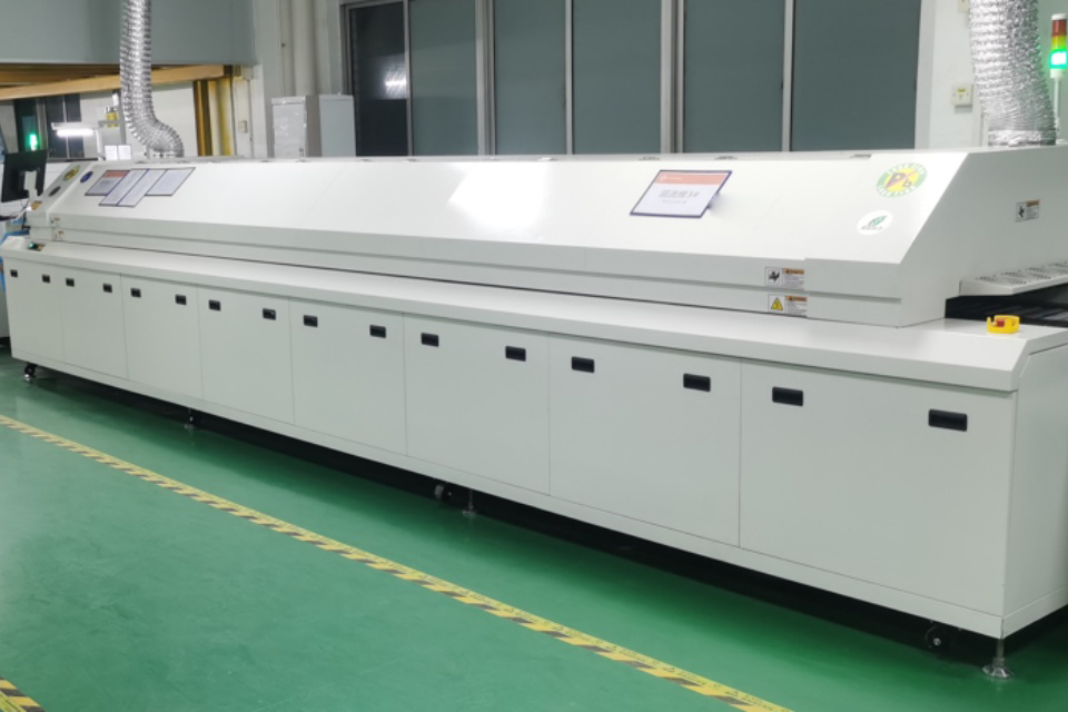
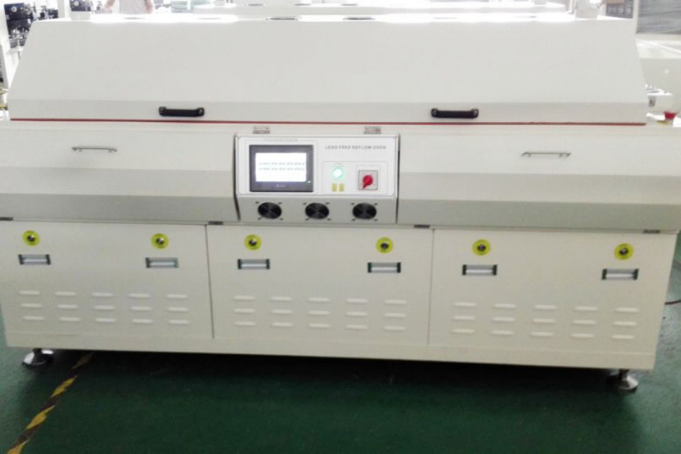
The phrase “component placement detection” gets thrown around like it means one thing. It doesn’t. There’s pre-placement detection inside the mounter, where the machine checks body shape, pickup offset, size, and rotation. Then there’s post-placement inspection—AOI, SPI-linked checks, 3D height comparison, sometimes X-ray—where the line asks, “Did reality match the program?”
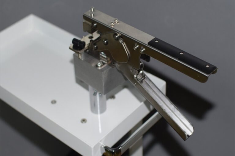
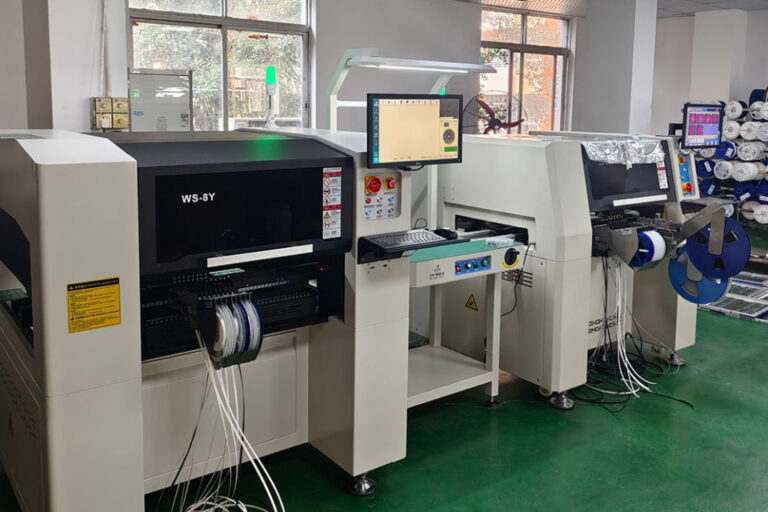
Modern pick and place machines don’t just grab parts and slam them onto FR-4. A decent machine checks feeder pickup, nozzle centering, package outline, θ angle, and correction values through upward-looking cameras or side optics. Yamaha YSM20R, Panasonic NPM-WX, Fuji NXT, Hanwha DECAN, Juki RS-series—different platforms, same religion: pick, image, correct, place.
But don’t worship the mounter.
A pick-and-place camera can catch geometry problems. It may catch a chipped corner or missing part. But subtle polarity? Low-contrast pin-one dots? A black molded IC with a barely visible laser mark? That’s where machine vision component orientation gets messy.
Why AOI Still Matters After Placement
Inline SMT inspection systems exist because the board changes after placement. Solder paste squishes. Components float. Dark packages sit on dark solder mask. Silkscreen polarity marks disappear under the package edge. A QFN that looked acceptable in the mounter can land with just enough skew to become a post-reflow headache.
I frankly believe too many shops still buy placement speed before process certainty. It’s macho procurement: CPH first, quality architecture later. Then everyone is shocked when the fast line makes bad boards at high speed.
Congratulations, you automated the mistake.
The serious factories treat orientation verification in manufacturing as a chain of custody. Not a feature. A chain.
Centroid file. BOM. Package library. Feeder table. Nozzle assignment. Fiducials. Upward camera. Board camera. AOI recipe. Operator response. MES traceability. Every link either protects the board or helps the defect sneak through.
Reuters offered a useful reminder in July 2024 when it reported that Nearfield Instruments raised USD 147.6 million for semiconductor metrology tools, with its CEO describing metrology as checking every manufacturing step against intent; Reuters also noted that advanced AI chips may require more than 2,000 process steps and that the advanced AI chip market was expected to grow 120% to roughly USD 110 billion that year. Nearfield raises $148 million (reuters.com)
No, PCB assembly is not wafer fab. But the principle travels well: the later you discover a bad process step, the more expensive the truth becomes.
NIST’s 2024 CHIPS Digital Twin Manufacturing USA material makes the same point in a more official voice, tying manufacturing progress to integrated materials, equipment, process, metrology/sensors, and AI/data analytics. CHIPS Digital Twin Manufacturing USA Institute (nist.gov)
That’s where automated component inspection is heading. Less “operator sees defect.” More “line sees drift.” Less screenshot theater. More feedback loop.
Where Real SMT Lines Usually Fail
For prototype and NPI work, the enemy is usually chaos. Substitute components, last-minute BOM changes, hand-edited centroid files, one-off panelization, odd polarity conventions from datasheets—this is where orientation mistakes breed. A good prototype and small-batch SMT line has to be built around first-article discipline, not just flexible feeders and a friendly UI.
From my experience, the first article is where the lies show up.
For high-volume production, the pain changes shape. The data may be stable, but drift becomes the killer. A tiny placement offset, feeder indexing issue, nozzle vacuum problem, or library rotation error doesn’t stay tiny when the line is making thousands of boards per shift. On high-speed mass production lines, a 0.3% orientation-related escape rate isn’t “low.” It’s a slow-motion product recall with better lighting.
That’s why better factories use feeder verification, reel barcode control, nozzle health checks, fiducial stability rules, AOI trend data, and stop conditions that actually stop the process.
Not suggest. Stop.
IPC’s industry page lists IPC-9716A, “Requirements for Automated Optical Inspection Process Control for Printed Board Assemblies,” along with IPC-9711 for automated inspection process control and IPC-HERMES-9852 for machine-to-machine communication in SMT assembly. IPC Industry Intelligence (shop.electronics.org)
That matters because the grown-up version of PCB component orientation detection isn’t a camera taking pretty defect photos. It’s process control. The AOI shouldn’t be a museum of mistakes. It should be a useful part of the factory nervous system.
Comparison: Detection Stages and Limits
The most dangerous orientation mistakes are usually boring. A diode stripe points the wrong way. A tantalum polarity bar is misread. A pin-one dot disappears under glare. A connector is mirrored because the library was copied from a sister product. A BGA looks symmetrical until the netlist says otherwise. A 01005 cap lands badly enough to tombstone during SAC305 reflow.
| Detection stage | Machine or method | What it catches well | What it often misses | My blunt rule |
|---|---|---|---|---|
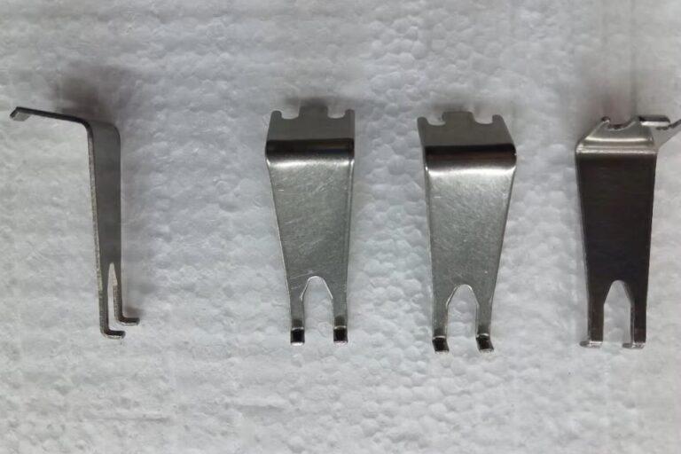
| Feeder setup verification | Barcode scanner, smart feeder, reel database | Wrong reel, wrong feeder slot, wrong part number | Incorrect component orientation inside tape pocket | Never run high-mix jobs without feeder traceability |
| Pre-placement vision | Upward-looking camera on pick-and-place machine | θ rotation, body outline, pickup offset, damaged or missing part | Subtle polarity marks, mirrored CAD assumptions | Good for geometry, not always enough for polarity |
| Fiducial correction | Board camera and CAD coordinate transform | Board shift, stretch, rotation, panel offset | Bad centroid data, wrong package library | Fiducials correct boards, not bad engineering |
| Inline AOI before reflow | 2D/3D AOI | Missing, skewed, reversed, offset, wrong package | Hidden solder joint defects under BGA/QFN | Best stop point before heat locks in the mistake |
| Post-reflow AOI | 2D/3D AOI | Tombstone, solder bridges, lifted leads, final polarity | Hidden voids, some bottom-termination defects | Necessary, but later than I like |
| X-ray inspection | AXI / X-ray | BGA, QFN, voiding, hidden joints | Visible polarity unless combined with optical data | Use when the joint is hidden, not as a bandage |
No single tool owns the truth.
Feeder verification catches the wrong reel, not always wrong tape orientation. Mounter vision catches geometry, not every polarity convention. AOI catches placement, but sometimes after value has already been added. X-ray sees hidden joints, but it won’t save sloppy front-end setup.
This is why I like turnkey SMT line solutions when specified properly. Not because “turnkey” sounds comforting—but because orientation detection works better when the printer, mounter, AOI, SPI, reflow, barcode system, and data layer are designed to talk.
A fast mounter feeding a blind inspection cell is not a quality system. It’s a gambling machine.
Lighting matters more than salespeople admit. Coaxial light can pull out laser marks. Low-angle ring light exposes leads. Structured light helps 3D AOI judge height and coplanarity. OCR can read package markings until the supplier changes font, contrast, molding compound, or marking location. Then your “AI inspection” starts acting like an intern on their second Monday.
I’m not anti-AI. I’m anti-magic.
Practical Rules for Correct Component Placement
Here’s how machines detect component orientation when the process is worth trusting: the placement program defines expected X, Y, and θ; the package library defines body, leads, pickup point, and polarity convention; fiducials correct the board coordinate frame; the mounter camera checks the live part; AOI checks the populated board; and the line records enough data to identify whether the problem came from a feeder, nozzle, package library, board stretch, or setup error.
How do you ensure correct component placement? Don’t start with the camera. Start with the source of truth.
Lock the BOM revision. Validate centroid export. Confirm pin one against the actual component, not just the PDF. Barcode the reel. Verify feeder slot. Check nozzle wear. Use upward-looking vision. Run first article like you’re trying to prove the program wrong. Put inline AOI before reflow where possible. Track false calls separately from escapes. And when a machine flags a polarity mismatch, don’t let an operator click through it because the shift target looks scary.
That click is where quality systems go to die.
For buyers comparing equipment, I’d ask uncomfortable questions. Can the system detect a 180° rotation on a low-contrast IC? Can it separate acceptable 0201 offset from feeder drift? Can the AOI recipe handle black-on-black packages? Does feeder data flow into inspection history? Can the engineer tune the recipe without creating a false-call swamp? Does the line stop, or does it merely complain?
Complaining is cheap.
A proper component orientation detection setup should make the factory quieter. Fewer arguments. Fewer heroic inspections. Fewer “who approved this build?” meetings. More boring green boards moving through the line because the process caught the dumb stuff early.
FAQs
What is component orientation detection?
Component orientation detection is the automated verification of a part’s rotation, polarity, pin-one position, body outline, and placement coordinates before or after it is mounted on a PCB, using machine vision, CAD data, feeder data, fiducials, and inspection rules to prevent reversed, skewed, missing, or incorrectly placed components. In SMT assembly, it’s the difference between a line that merely places parts and a line that knows whether those parts make sense.
How do machines detect component orientation?
Machines detect component orientation by comparing live component or board images against programmed references that include centroid coordinates, θ rotation, package geometry, polarity markings, pin-one features, fiducial correction, and acceptance tolerances for skew, offset, body size, and lead position. The check may happen inside the pick-and-place machine, at inline AOI, or across both systems when the line is properly integrated.
Is AOI enough to prevent wrong component placement?
AOI is not enough by itself because it usually detects wrong component placement after the placement event, while the strongest control system prevents obvious rotation, pickup, feeder, and package errors before the part ever touches the PCB. AOI still matters, but it should sit inside a broader setup that includes feeder verification, machine vision, first-article review, and process feedback.
Which components need orientation verification most?
Orientation verification matters most for polarized or pin-indexed devices such as diodes, LEDs, electrolytic and tantalum capacitors, connectors, SOICs, QFPs, QFNs, BGAs, and ICs with pin-one markings, because a 90° or 180° error can create immediate functional failure or latent field risk. Non-polar passives can still cause trouble when poor placement geometry leads to tombstoning, skew, or weak solder joints.
How can manufacturers ensure correct component placement?
Manufacturers ensure correct component placement by controlling the full chain: clean centroid data, verified feeder setup, calibrated nozzles, reliable fiducial recognition, validated polarity libraries, upward-looking camera checks, inline AOI, first-article inspection, and SPC feedback that stops drift before it becomes repeat scrap. The best shops don’t treat inspection as a final exam; they use it as live process feedback.
Build a Line That Stops Orientation Errors Early
If your SMT line keeps finding orientation errors after reflow, you don’t have a “small inspection issue.” You have a process leak.
Start with the architecture, not the brochure: compare SMT inspection systems, review your feeder and placement workflow, then use the contact page to discuss a line setup that catches wrong orientation before it becomes someone’s failure-analysis problem.