Most teams miss it.
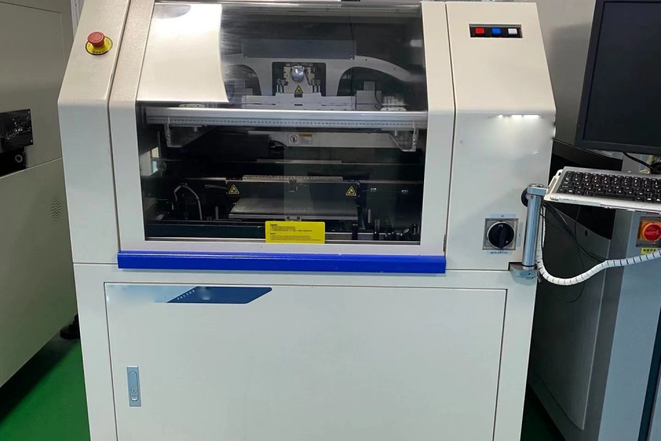
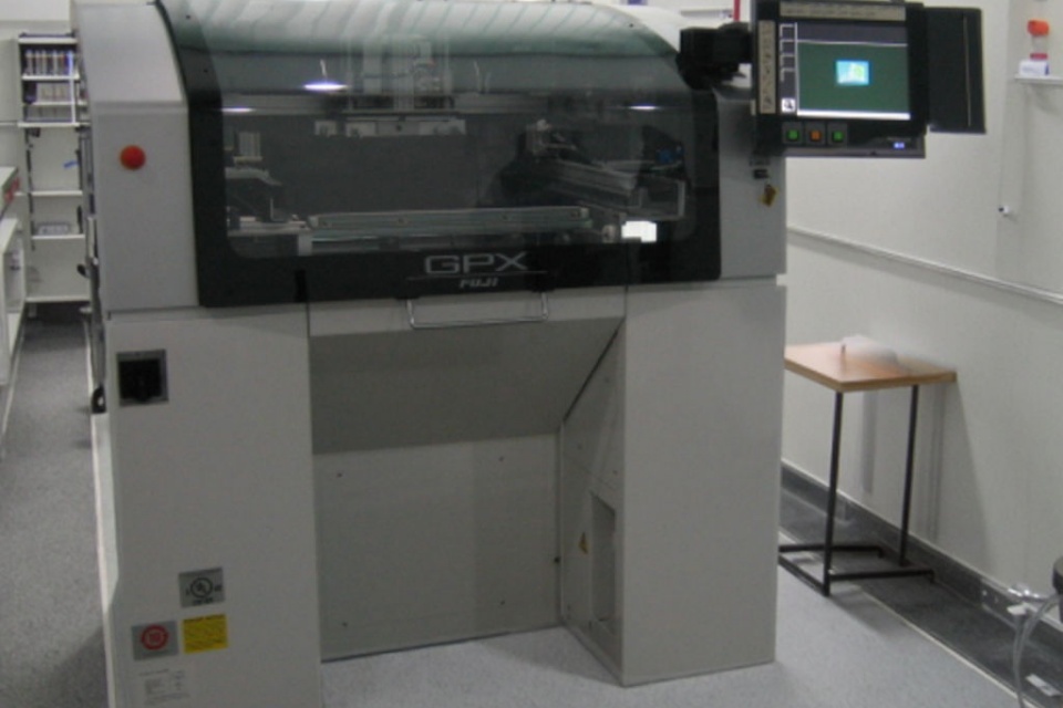
When people talk about design for testability, they usually drift toward in-circuit test, flying probe access, or boundary-scan checklists, but on a live SMT floor the nastier question arrives first: can the placement head, feeder setup, vision system, AOI recipe, repair tech, and quality engineer actually see, reach, and verify the board you designed without guessing? What else do you think “testability” means when the defect starts at placement, not at final electrical test?
My blunt view is this: most DFT PCB discussions are too electrical and not physical enough. A 2024 Springer survey on automatic PCB inspection underscored that visual inspection methods dominate modern PCB inspection, that AOI remains the most practical fast and non-destructive method, and that assembled boards are harder than bare boards because component variety and design churn create far messier inspection conditions. (Springer)
So here is the hard truth. If your board hides fiducials, buries polarity marks, crowds tall parts against small passives, gives AOI no clean sight line, and leaves no sane way to map feeder data to a board serial number, your so-called design for testability is cosmetic. It might pass a slide deck. It will not pass a line audit.
The standards side is not vague, either. The 2024 ANSI overview of IPC-A-610J-2024 notes that IPC-A-610 remains the most widely used electronics-assembly acceptability standard and explicitly ties acceptability to related design, land-pattern, and soldered-assembly documents such as IPC-222x, IPC-7351B, and J-STD-001J-2024. That matters because pick and place verification is not separate from quality acceptance; it is where quality acceptance starts. (The ANSI Blog)
Accessibility is physical, optical, and data-level
Physical access comes first. If a nozzle cannot place cleanly, if a camera cannot view reference features, if a rework tool cannot reach a suspect QFN or 0201 cluster, you do not have accessibility for PCB testing; you have layout vanity.
Optical access comes next. Pick and place verification lives on contrast, orientation, readable markings, stable fiducials, and unobstructed views. A polarity stripe hidden under a can, a reference designator clipped by solder mask art, or a local fiducial shadowed by a tall electrolytic is not a minor nuisance. It is an invitation to false confidence.
Then comes data access. I keep seeing teams obsess over centroids but ignore traceability architecture. That is backward. Verification is stronger when feeder ID, reel lot, nozzle event, board serial, AOI image, and repair record can be connected fast, without detective work, across setup, placement, inspection, and debug.
And no, this is not theory. In a 2024 Hyundai rearview camera recall report, NHTSA said 1,760 U.S.-market vehicles were affected because insufficient solder joints on the camera PCB could worsen over time and cause failure of the rearview image. In Audi’s 2024 69GU safety recall, the problem was pins not soldered correctly to the circuit board in a passenger-seat occupant detection control module, with a potential airbag consequence. Then regulators went a step further: in November 2024, NHTSA’s consent order with Ford imposed a $165 million civil penalty over delayed rearview-camera recall compliance and required VIN-level traceability plus a low-voltage electronics imaging lab. That is the part too many factories still refuse to hear: weak verification eventually stops being an internal quality issue and becomes a legal and regulatory one.
If you build or sell SMT capability, this conversation belongs beside your process and quality work, your choice of SMT inspection systems, the limits of your pick-and-place machines, and the production logic behind turnkey automation. And if anyone on the team insists these failures are hypothetical, point them to real-world customer cases instead of another polished brochure.
What good DFT PCB work actually changes
A serious DFT PCB strategy makes verification cheaper before it makes testing smarter. It reduces ambiguity. It shortens first-article approval. It lowers the number of “possible wrong part” calls that end up being camera noise, bad markings, or inaccessible geometry. It also speeds failure containment when something is wrong, because the board was designed for visibility, not just density.
That last point matters more than people admit. The industry still rewards layout density like it is a moral virtue. I do not buy that. A board that saves 4 mm of area and costs you hours of setup friction, AOI tuning, debug delay, and rework pain is not efficient. It is merely compact.
Here is the shop-floor version of the argument:
| DFT choice | What verification needs | What happens when it is ignored | Better move |
|---|---|---|---|
| Global and local fiducials | Stable reference points with clean camera view | Offset drift, bad teach, weak first-article confidence | Place fiducials where vision can actually see them in dense zones |
| Clear polarity and orientation marks | Unambiguous visual confirmation after placement | Reversed diodes, electrolytics, IC orientation mistakes | Keep markings visible after the part is mounted |
| Component spacing around tall and tiny parts | Nozzle clearance and AOI sight lines | Shadowing, false calls, skipped or misread parts | Design for line-of-sight, not just nominal placement clearance |
| Test pads and debug access | Fast confirmation when placement is suspected | Low coverage, slow isolation, expensive rework loops | Reserve access during layout, not after routing is frozen |
| Board ID and traceability fields | Clean readable mapping from reel to board | Hard containment, ugly root-cause hunts | Tie serial, feeder, lot, and inspection records together |
| Rework corridors | Practical access for microscope, hot air, and hand tools | “Passes build, fails service” boards | Leave recovery space around high-risk parts |
How to improve pick and place verification without slowing the line
Start with reference integrity. If the centroid is right but the fiducial strategy is weak, the machine is working from shaky truth. That is not precision. That is automation with better posture.
Then fix human-readable confirmation. A DFT PCB should let an operator, programmer, and auditor answer three fast questions: Is it the right part? Is it rotated correctly? Can I prove it on this exact board revision? If the answer depends on tribal memory, your process is not robust.
Then protect inspection sight lines. The 2024 Springer review makes the uncomfortable point that PCBA inspection is harder than bare-board inspection because the object itself is more complex and changes more often. So when layout teams stack dense parts, mixed heights, reflective surfaces, shields, and ambiguous markings into one field of view, they are not challenging AOI to “get smarter”; they are feeding it garbage. (Springer)
And yes, machine capability matters. Verification rules should be written against the actual line: feeder type, camera resolution, nozzle family, board support method, and AOI library behavior. That is why generic PCB testability guidelines so often fail in production. They are written like commandments. Lines do not run on commandments. They run on constraints.
The part nobody says in meetings
Here it is.
Design for testability is really design for evidence. Not hope. Not operator heroics. Not “the machine should catch it.” Evidence.
If your board cannot produce fast evidence at setup, at placement, after placement, after reflow, and during debug, you have built a board that depends on luck. And luck is a terrible quality system.
That is why I treat accessibility for PCB testing as a first-order design variable, not a cleanup item. In practice, it means visible fiducials, readable polarity, inspectable spacing, reachable suspect joints, and traceability that survives lot splits, feeder swaps, and revision changes. It also means accepting an unpopular fact: sometimes the best DFT practices for PCB assembly look less elegant in CAD and much better in production yield.
FAQs
What is design for testability in PCB assembly?
Design for testability in PCB assembly is the practice of designing the board, markings, access points, and production data so machines and people can verify component identity, orientation, solder quality, and traceability quickly across setup, placement, inspection, debug, and repair. In plain English, it is the difference between proving a board is right and merely hoping it is right. (The ANSI Blog)
What is accessibility for pick and place verification?
Accessibility for pick and place verification is the board’s built-in ability to let placement heads, vision systems, AOI programs, and technicians physically reach, optically see, and digitally confirm what was loaded, placed, and soldered, without hidden marks, blocked sight lines, or ambiguous reference data. If any one of those access paths is broken, verification quality drops fast. (Springer)
What are the best DFT practices for PCB assembly?
The best DFT practices for PCB assembly are early test-pad planning, unambiguous polarity marking, fiducials with clean camera views, readable traceability IDs, rework clearance around risky components, and inspection rules matched to the actual machine set rather than an abstract CAD ideal. The stronger version of that answer is simple: design for visibility before you design for density. (The ANSI Blog)
How do I improve pick and place verification on a real SMT line?
To improve pick and place verification, reduce ambiguity before the board hits the line: make reference coordinates stable, marks visible after assembly, feeder mapping traceable, component spacing inspectable, and post-placement confirmation fast enough that first-article approval catches errors before they multiply across the lot. The winning move is earlier evidence, not more late-stage firefighting. (Springer)
If your team is serious about reducing wrong-part calls, polarity escapes, and slow debug, review the board against your actual process and quality workflow, benchmark it against the capabilities of your SMT inspection systems and pick-and-place machines, and then contact the team before the next revision locks in another avoidable blind spot.