Fiducials aren’t optional. They’re the quiet referee that tells the machine what “zero” means when your PCB shows up slightly rotated, slightly shifted, slightly bowed, and sometimes slightly shiny in a way the camera hates.
I’ve watched smart teams waste days “tuning” a pick and place machine alignment issue that was never a machine issue. It was a board issue. The fiducials were tiny, crowded by silkscreen, sitting near copper pour noise, and the solder mask opening looked like it got chewed by a dull bit.
So what’s really going on?
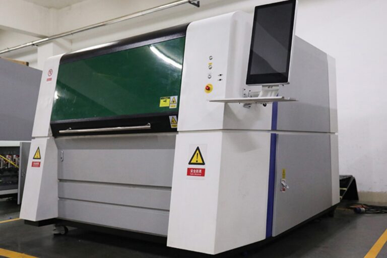
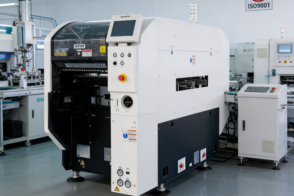
A pick-and-place doesn’t “align to your CAD.” It aligns to pixels. It aligns to contrast. It aligns to whatever the SMT vision system alignment algorithm can reliably lock onto at 30,000+ CPH while the conveyor is still vibrating.
And yes, the industry still underestimates how hard that is.
What PCB fiducial marks actually do (and what they don’t)
Here’s the ugly truth: the machine never fully trusts the board. It trusts math.
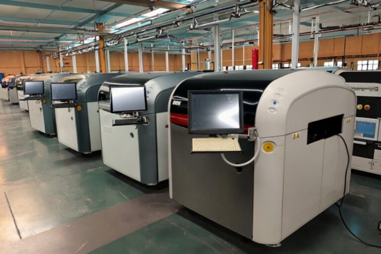
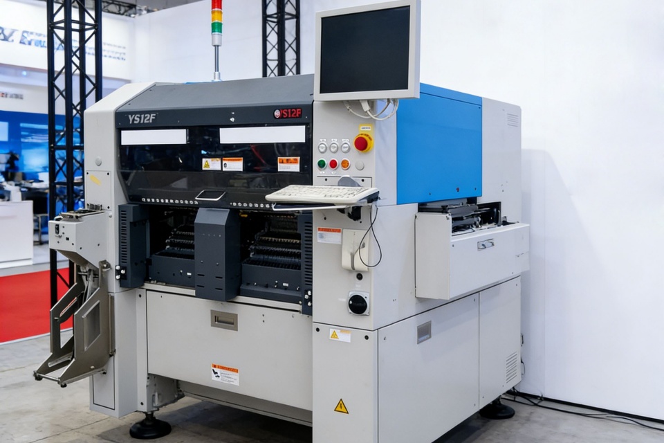
A typical placement workflow looks like this, whether you’re running a Yamaha, Fuji, Panasonic, ASM, Hanwha, JUKI—pick your badge:
- The board enters, clamps, and gets a quick “where are you?” capture.
- The camera searches for PCB registration marks (fiducials).
- The software solves translation (X/Y) and rotation (θ) from at least two points.
- Better systems also estimate slight scaling/shear using extra marks (that “board stretch compensation” feature people brag about in demos).
- Then placement starts… and keeps correcting.
Simple? Not really. Because the fiducial image is rarely perfect.
Glare happens. Mask misregistration happens. Dust happens. Warp happens. And when the fiducial is poorly designed, the camera spends extra milliseconds hunting—then your line speed drops, and everyone pretends it’s feeder related.
If you want the boring promise in writing, your supplier should put it in a policy like a service promise for SMT equipment support, not just a sales deck.
Why designers keep getting fiducials wrong
Because fiducials don’t look like “real circuitry.” So they get shoved into the corner at the end. Then the PCB comes back panelized, rails added, V-scores moved, and your “corner” is no longer a corner.
Also, layout teams optimize for routing density. The line optimizes for visual certainty. Those goals fight each other.
Want proof that vision quality is a real research problem, not a “just add fiducials” checkbox? A 2023 PubMed-indexed paper on fiducial mark segmentation reported measurable accuracy gains from a modified U-Net approach (mARU-Net) specifically because real fiducials sit in messy, high-noise backgrounds. That’s not hobby work. That’s factories pushing vision to behave. PubMed record for the study. (PubMed)
Fiducial mark placement guidelines I actually trust
Three words: make it easy.
Now the detailed version, because “easy” has specs:
- Use global fiducials: at least 2, ideally 3, far apart. Put them near opposite corners of the board (or panel rails, if that’s what the machine sees first).
- Add local fiducials for fine-pitch and dense areas: BGAs, 0.4 mm pitch QFNs, µBGAs, tight connector zones.
- Keep them clean: no silkscreen, no text, no solder paste, no via in keepout.
- Control geometry: round copper pad, solid edge, consistent finish.
- Give clearance: solder mask clearance and copper keepout are not “nice-to-have.” They’re the difference between a crisp target and a smeared blob.
And yes, I’ll say it: if you’re running tiny passives (01005 is 0.4 × 0.2 mm) and still using “one fiducial near the logo,” you’re gambling with yield.
Global fiducials vs local fiducials: stop treating this like a debate
It’s not religion. It’s error budgeting.
Global fiducials fix board-level position and rotation. Local fiducials reduce residual error near a critical placement zone—especially when the board warps, the panel flexes, or you have accumulated tolerance from depaneling.
If you run mixed work (prototype today, volume tomorrow), design for both. If you need a line that can switch gears without drama, look at prototype and small-batch SMT line solutions and also high-speed mass production SMT lines—because the fiducial strategy that “works” at 2,000 CPH can fall apart at 35,000 CPH when the vision cycle time becomes the bottleneck. (Pick and Place Machine)
Fiducial mark size and clearance: the numbers people keep hand-waving
I’m going to be practical here.
Most assemblers I respect are happy with something in this neighborhood:
- Copper pad diameter: ~ 1.0 mm (often acceptable range: 0.8–1.5 mm)
- Solder mask opening: ~ 2.0–3.0 mm (you want a clean “ring” of non-mask around it)
- Keepout (no copper features, no silkscreen, no vias): roughly 2.0–3.0 mm around the fiducial edge, depending on camera field-of-view and your assembler’s rules
But. And this matters. The “best” numbers depend on the camera setup: lens type (telecentric vs standard), lighting (coaxial vs ring), and detection method (edge-detect vs pattern matching vs ML-based segmentation). That’s why serious teams align DFM rules with the specific line, not generic internet charts.
If you want fewer surprises, bake this into your process documentation and training. A vendor that sells you a turnkey line should also offer training and after-sales support, because half of alignment pain is operator setup and half is PCB design habits. (tsapps.nist.gov)
The “fiducial visibility” problem nobody wants to admit
Cameras don’t see “copper.” They see contrast. So surface finish matters.
ENIG can glare under certain lighting. OSP can look flatter. HASL can look uneven at the edge. None of this is fatal—unless your fiducial is tiny and crowded and the mask opening is sloppy. Then the vision system starts guessing.
And guessing is expensive.
This is why I don’t roll my eyes when people bring up measurement and perception research. NIST put out a 2024 report on measurement science needs for manufacturing robotics, explicitly calling out perception/machine vision as a core technical need while factories adopt more automation under labor and cost pressure. NIST GCR 24-054 (June 2024). (tsapps.nist.gov)
A comparison table you can hand to a PCB designer
| Topic | Global Fiducials | Local Fiducials | What I’d do in real life |
|---|---|---|---|
| Purpose | Board-level X/Y/θ alignment | Fine alignment near critical parts | Use both on any “serious” board |
| Count | 2 minimum, 3 preferred | 1–2 per dense zone | 3 global + locals for BGA/QFN zones |
| Placement | Far apart, near corners/rails | Close to the component cluster | Keep locals within ~25–50 mm of target area when possible |
| Risk if wrong | Whole board shifts/rotates | Only one region drifts | Global errors kill yield fast |
| Design pitfalls | Hidden by rails, silkscreen, copper pour | Put inside keepouts, too close to pads | Lock rules in CAD, don’t “eyeball” it |
| Best use case | Any PCB assembly | Fine pitch, high density, warped panels | Mixed SMT lines, tight tolerances |
Real-world pressure: why this matters more in 2024 than it did in 2014
Automation money is flowing. That’s not a vibe. It’s capital.
Reuters reported in June 2024 that Bright Machines raised $106 million in a funding round involving Nvidia and Microsoft, explicitly focused on automating manufacturing tasks with AI and computer vision. That tells you where the industry thinks the pain is: labor, speed, consistency. Reuters coverage. (Reuters)
But here’s the part people miss: even as AI gets layered in, fiducials remain the low-level truth anchor. You can’t “AI your way” out of bad targets. You just build a smarter system that fails more gracefully—after you’ve already paid for the complexity.
Also, robotics research is getting sharper on precision handling. MIT’s 2024 write-up on SimPLE (Science Robotics) highlights pick-and-place methods chasing high placement success rates across varied objects, because precision is still the hard part in real deployments. MIT News (Aug 9, 2024). (news.mit.edu)
So yes, your fiducial rules matter. More than ever.
The internal process fix most companies avoid
You need one owner. Not “everyone.”
In good factories, PCB fiducial marks are part of the release checklist, not a tribal memory. The DFM reviewer checks: global count, spacing, mask clearance, keepout, panel rail impact, and whether local fiducials exist where they’re needed.
If you’re buying equipment or rebuilding a line, do it as a system. That’s why turnkey SMT line solutions exist in the first place: printer + placement + reflow + inspection + handling, tuned together, not Frankensteined from “best deals.” (tsapps.nist.gov)
FAQs
How do PCB fiducial marks help pick and place machines align PCBs?
PCB fiducial marks are exposed reference targets that a pick-and-place camera measures to compute the board’s X/Y shift and rotation angle, then apply that correction to every placement coordinate during the build. They turn a drifting, imperfect conveyor world into a stable coordinate system the machine can trust.
After that definition, here’s the practical bit: two marks solve position and rotation; extra marks help compensate for slight stretch, panel flex, or localized distortion near dense parts. If your line places 01005 or 0.4 mm pitch parts, locals near the hot zone often save real yield.
What are fiducial mark placement guidelines that reduce placement errors?
Fiducial mark placement guidelines are layout rules that position clean, high-contrast fiducials (global and local) so the SMT vision system can detect them quickly and repeatably without interference from silkscreen, copper features, vias, or solder mask artifacts. The goal is fast detection and low false-lock risk across many boards.
In practice: put 2–3 global fiducials far apart, keep generous mask clearance, keep a feature-free keepout around each mark, and add local fiducials near fine-pitch clusters. Don’t bury fiducials in rails that get modified by panelization.
Global fiducials vs local fiducials: which one matters more?
Global fiducials vs local fiducials is a question about which error you’re trying to control: global fiducials correct whole-board offset and rotation, while local fiducials reduce residual misalignment near a specific component region when warp, flex, or tolerance stack-up creates local drift. Both serve different parts of the same alignment problem.
If you only pick one, global wins because it sets the base coordinate system. But if you’re placing tight-pitch BGAs or micro parts, locals often prevent the “everything looks fine except this corner” failure that makes engineers blame feeders, nozzles, or paste.
What fiducial mark size and clearance should I use for SMT vision?
Fiducial mark size and clearance refers to the copper pad diameter and the surrounding solder mask opening/keepout region that ensures the camera sees a crisp circular target with strong edge contrast and minimal background noise. The right sizing avoids glare, mask encroachment, and false edges that slow detection.
Common factory-friendly starting points are ~1.0 mm copper with a 2.0–3.0 mm solder mask opening and a feature-free keepout around it, but your assembler’s rules and camera setup can shift that. When in doubt, match the line’s proven DFM rules instead of guessing.
Are PCB registration marks the same as fiducials?
PCB registration marks are reference features used to align processes, and in SMT assembly that usually means fiducial marks: exposed targets used by optical systems for board alignment in printing, placement, and sometimes inspection. People use the terms loosely, but “fiducial” is the specific SMT vision target most lines rely on.
You’ll also hear “tooling holes” in the same conversation. Tooling holes help mechanical handling and coarse alignment; fiducials handle optical precision. Mixing them up causes bad decisions.
Why does pick and place machine alignment fail even with fiducials present?
Pick and place machine alignment can fail even with fiducials because the camera may not reliably detect the targets due to glare, solder mask misregistration, silkscreen overlap, copper pour clutter, contamination, panel rail changes, or fiducials placed too close together to stabilize rotation math. “Has fiducials” isn’t the same as “has detectable fiducials.”
If the vision algorithm locks onto the wrong edge or a dirty target, the correction is wrong, and every placement shifts consistently. That’s why the fix often lives in PCB design rules and panelization control, not in another hour of machine parameter tweaking.
Conclusion
If you want the fastest way to stop arguing about alignment, let’s look at your Gerbers and your line goals together. Use contact our SMT team and tell us what you’re building (component sizes, pitch, panel format, target CPH). If you’re scaling up, start with turnkey SMT line solutions so the printer, mounter, handling, and inspection agree on one coordinate reality—because your fiducials can’t fix a line that fights itself.