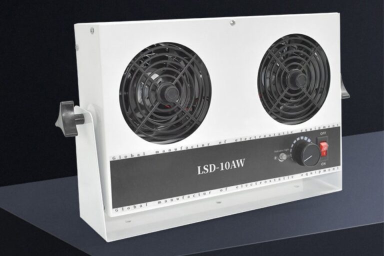
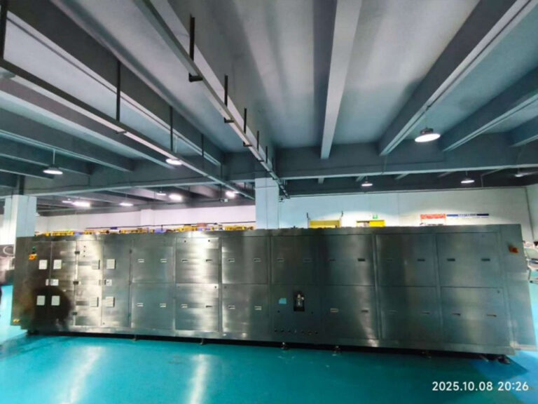
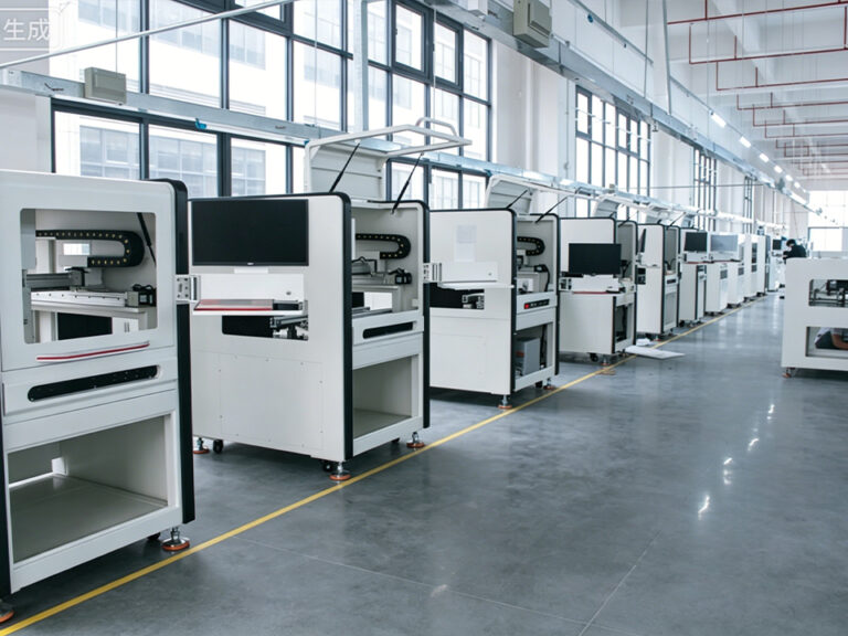
Placement accuracy does not stop a package or PCB from bending during reflow. It preserves enough terminal-to-paste overlap for the solder joint to survive that movement.
That distinction matters.
Many factories find head-in-pillow defects, corner-ball opens, or QFN edge failures and immediately blame the reflow oven. But placement offset, solder-paste registration, board support, and package warpage often interact.
A practical model is:
Joint margin = initial overlap + solder collapse − placement offset − package lift − board movement
Every micrometre lost through placement error reduces the margin available to absorb thermal deformation.
What Causes Components to Warp During Reflow?
Component and PCB warping occurs because silicon, copper, laminate resin, mold compound, solder mask, and package substrates expand at different rates.
Common causes include:
- Coefficient-of-thermal-expansion mismatch
- Asymmetric package or PCB construction
- Uneven copper distribution
- Excessive heating or cooling rates
- Moisture absorption
- Thin boards or large packages
- Poor board support
Warpage is dynamic. A package may be convex at room temperature, flatten during heating, become concave near peak temperature, and retain residual deformation after cooling.
This means room-temperature flatness alone cannot predict reflow behaviour.
Why Placement Precision Matters
Molten solder can self-align a component, but only when paste volume, wetting, pad geometry, terminal contact, and component movement remain balanced.
If a warped BGA corner lifts away from the paste, solder cannot pull it back into contact. If a QFN is rotated or shifted before reflow, deformation can reduce terminal overlap further. Small passive components may also skew or tombstone when placement depth and paste contact are unequal.
A component can remain within the placement machine’s general tolerance while still falling outside the solder joint’s safe process window.
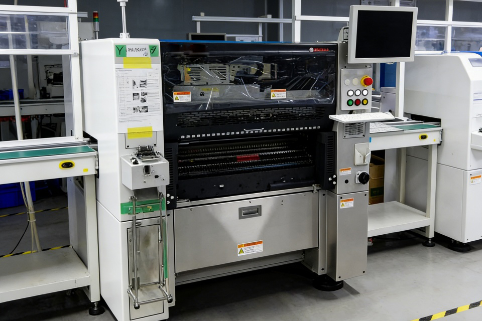
Placement Controls That Reduce Warpage-Related Defects
Use Package-Specific Tolerances
Do not apply one placement tolerance to every component.
A 40 µm offset has very different consequences for an 01005 resistor, a 0.4 mm-pitch BGA, a QFN, or a large connector.
Control:
- X and Y offset
- Theta rotation
- Placement height
- Placement force
- Nozzle condition
- Recognition accuracy
- Local board height
Track the full distribution, not only the average. A good mean result can hide occasional large deviations that cause failures.
Recognise the Electrical Interface
Package bodies are not always perfectly centred over their leads, balls, or terminals.
For BGAs, CSPs, LGAs, and leadless packages, use bottom-side, ball, or lead recognition where possible. Body-edge recognition may centre the plastic package while leaving the solderable terminals misaligned.
Control Placement Force
Excessive force can squeeze paste unevenly, tilt components, or deflect thin boards. Too little force may leave terminals resting on inconsistent paste peaks.
Support pins should be positioned around high-force, heavy, or warpage-sensitive components rather than placed only where space is convenient.
Connect SPI and Placement Data
Solder-paste inspection and placement records should use common component IDs and board coordinates.
For each defect, engineers should be able to review:
- Paste volume and height
- Paste centroid offset
- Placement X, Y, and theta
- Nozzle and feeder identity
- Board support configuration
- Reflow recipe
- AOI or X-ray results
An integrated SMT denetim sistemi helps determine whether the failure began during printing, placement, reflow, or inspection.
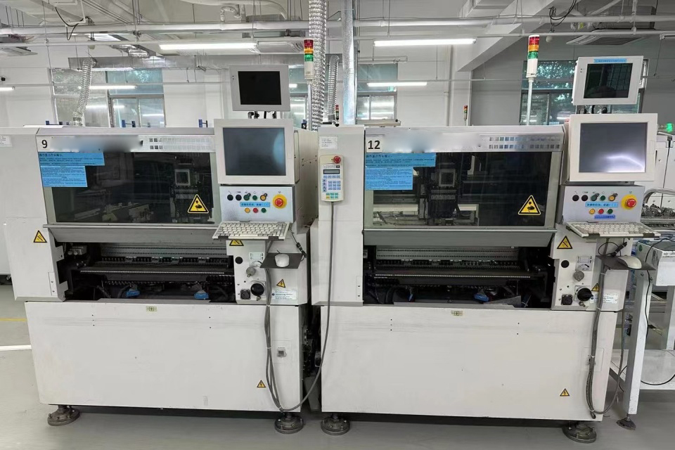
Common Failure Signatures
| Failure | Warpage effect | Placement contribution | Best inspection |
|---|---|---|---|
| BGA head-in-pillow | Corner lift separates ball from paste | Offset reduces contact area | X-ray, cross-section |
| BGA corner open | Local gap increases during heating | Poor centring reduces overlap | X-ray and placement-data review |
| QFN edge open | One edge lifts from the PCB | Rotation moves terminals toward pad limits | X-ray or cross-section |
| Tombstoning | Unequal wetting lifts one end | Unequal depth or paste contact increases imbalance | SPI and AOI |
| Bridging | Collapse pushes solder sideways | Offset concentrates solder on one side | X-ray and paste-volume analysis |
| Connector bow | PCB movement shifts joint rows | Placement error increases cumulative misalignment | Board-height mapping and X-ray |
Profile the Actual Assembly
A reflow recipe is not validated simply because the oven display matches its setpoints.
Use a calibrated yeniden akış termal profilleyici on the populated board and measure:
- Ramp rate
- Soak time
- Time above liquidus
- Peak package temperature
- Temperature differences across the board
- Cooling rate
Repeat profiling with the real conveyor speed, rail width, support tooling, board orientation, nitrogen setting, and production load.
The selected yeniden akış fırını should provide stable airflow, adequate zone control, reliable board support, and consistent thermal recovery.
Best Component Placement Practices for Reflow
Start by identifying thin, fine-pitch, large, heavy, or historically unstable packages.
Then:
- Measure placement capability by package and board location.
- Compare paste and component centroids.
- Support the board beneath sensitive areas.
- Profile the populated assembly.
- Use X-ray for hidden joints.
- Test placement, support, paste, and thermal changes separately.
Changing every process variable at once may improve yield, but it prevents engineers from identifying the actual cause.
Sıkça Sorulan Sorular
What causes components to warp during reflow?
Component warping during reflow is the thermal bending or twisting of a package, PCB, or both because their materials expand, soften, and cool at different rates.
CTE mismatch, uneven copper, moisture, package construction, rapid heating, and poor board support are common causes.
How does placement precision prevent reflow defects?
Placement precision keeps component terminals aligned with solder paste and PCB pads, preserving the contact area needed when the component or board moves during heating.
It does not eliminate warpage. It reduces the likelihood that warpage will create an open, bridge, or head-in-pillow defect.
Which defects indicate warpage?
Warpage-related defects commonly include head-in-pillow, corner-ball opens, QFN edge opens, intermittent BGA joints, bridging, skew, and tombstoning.
Repeated failures at package corners or along one edge are strong warning signs.
Should reflow temperature be lowered?
Lowering reflow temperature may reduce deformation, but only when the solder alloy, flux, wetting, time above liquidus, and reliability requirements remain satisfied.
A cooler profile that produces incomplete wetting is not an improvement.
Stop Treating Warpage as an Oven-Only Problem
Reliable prevention requires accurate placement, balanced paste deposits, effective board support, controlled thermal gradients, and inspection of hidden solder joints.
Factories should not ask only which machine is fastest. They should ask which process leaves the greatest joint margin when the package and PCB stop being flat.
Review available Anahtar teslim SMT hattı çözümleri veya contact an SMT engineer to evaluate placement, profiling, support, and inspection requirements.