Boards mislead people.
I’ve seen a line stop over what looked like one dumb solder bridge on a fine-pitch QFP, only to find the real mess sitting three stations upstream—stencil wear nobody logged, a humidity spike nobody respected, and a reflow recipe that had already chewed through the process window before the first operator even called MRB. It happens. More than people admit.
And that’s the problem, isn’t it?
Too many teams still talk about PCB repair like it’s some noble rescue mission. I frankly believe that mindset causes more damage than the defect itself. Because once the bench tech becomes the hero, process discipline usually becomes the victim. You stop asking why the board failed and start admiring how cleverly someone patched it.
Bad trade.
So I start with the ugly stuff first: money, liability, field risk. Not bench pride. The Global e-Waste Monitor 2024 says the world generated 62 million tonnes of e-waste in 2022, only 22.3% was documented as properly collected and recycled, and about $62 billion in recoverable resources effectively slipped away; the report also points to short lifecycles and weak repairability as part of the story, which should bother anyone pretending discard is always the cleanest answer. That number sticks. (unitar.org)
But don’t romanticize recovery either.
A 2024 University of Washington team reported a vitrimer-based PCB design that can be recycled repeatedly while still performing like conventional boards, which, to me, lands like a warning shot: the future is not “use it once and move on,” and factories that keep treating boards as disposable line items are going to look dated fast. That’s where this is heading. (washington.edu)
Here’s the ugly truth: if your PCB rework program is busy every day, your yield program is lying to you.
Rework isn’t repair, and scrap isn’t weakness
People blur these terms constantly.
The 2024 IPC-7711/21 Revision D guide doesn’t blur them. It lays out rework, repair, modification, and disposition as separate decisions, and it does something a lot of production managers hate—it forces the conversation back to product class, failure context, and whether the assembly is being corrected in manufacturing or after service use. That difference matters. A lot. (shop.ipc.org)
Let me say it straight.
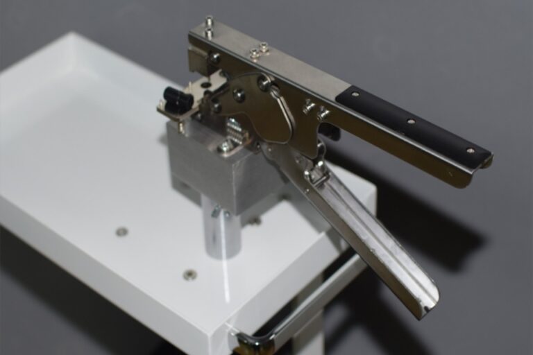
PCB rework means restoring the assembly to the intended build condition. Wrong resistor? Swap it. Skewed SOIC? Remove and reinstall. Solder bridge on a gull-wing lead? Fine—fix it, inspect it, test it, move on. Board-level repair is a different animal. Now we’re talking lifted lands, trace reconstruction, barrel damage, jumper wires, laminate injury, maybe pad cratering if somebody got too enthusiastic with heat or pry force. That’s not “tidy up the board.” That’s surgery.
And scrap? Scrap is not failure. Scrap is often the first honest decision made all day.
IPC’s 2024 document makes that painfully clear by covering invasive actions like BGA work, plated-hole repair, lifted-land repair, surface-mount pad restoration, and jumper-wire methods—while also framing discard as a legitimate outcome, not some moral defeat. That’s a mature standard. Factories should act like it. (ipc.org)
The recovery ladder I actually trust
I don’t ask, “Can a tech make this board pass?”
Wrong question.
I ask whether the defect is isolated, whether the thermal budget is still intact, whether the board will hold up outside the lab, and whether the team has proof—not bench folklore—that the repair won’t turn into a latent field return six months later after a few thermal cycles and a bit of vibration. That’s the real test.
| Defect pattern | Best recovery move | I greenlight it when | I stop and scrap when |
|---|---|---|---|
| QFP bridge, insufficient wetting, 0402 tombstone | Localized PCB rework | Root cause is isolated and upstream print/profile control is stable | Same defect repeats across lot or heat exposure is stacking |
| Wrong polarity or wrong component installed | Controlled rework and retest | No pad damage, no trace lifting, no latent overstress | Sensitive ICs or nearby parts have likely seen damaging thermal or electrical abuse |
| Single BGA open or head-in-pillow suspicion | Targeted BGA rework | X-ray, profile history, moisture handling, and post-rework validation are all in place | Package warpage, pad damage, repeated BGA touch history, or Class 3 risk |
| Lifted pad or damaged land | Board-level repair | Net is repairable, geometry can be restored, and product class allows it | Fine-pitch density, RF/high-speed sensitivity, or anchor strength cannot be restored confidently |
| Via/barrel damage | Plated-hole repair or engineered jumper | Electrical and mechanical performance remain acceptable after repair | Current load, impedance control, or multilayer risk makes the repair guesswork |
| Ionic contamination, corrosion, moisture attack | Cleaning plus failure analysis first | Contamination is superficial and conductors remain intact | Corrosion has migrated under components or through porous board structures |
| Same-location failure across multiple boards | Line stop, not bench heroics | Never as a first response | Always investigate process before more repair |
I know that table feels harsher than what some production meetings want to hear. Good. It should. IPC’s own structure points to exactly this sort of disposition discipline—it treats “use as-is,” “repair,” “rework,” and “discard” as decision branches, not emotional reactions. (ipc.org)
Three cases that should kill the fairy tale
But let’s get out of theory for a second.
In Honda’s 2024 NHTSA recall report, a capacitor in the printed circuit board of the front passenger seat weight sensor could crack and short because of humidity exposure, after a supplier temporarily changed the PCB base material following a natural disaster; by January 25, 2024, Honda had already logged 3,834 warranty claims, and the fix was replacement with units built using the original approved material. That’s not a soldering problem. That’s governance failure dressed up as sourcing flexibility. NHTSA recall report 24V-064 (static.nhtsa.gov)
And people still say material substitutions are harmless?
The March 16, 2023 CPSC recall for STIHL iMOW docking stations hit about 2,700 units because the printed circuit board could short when exposed to moisture. That sentence should make every electronics manufacturer wince. Moisture ingress is boring right up until it starts fires. Then it’s not boring anymore. (cpsc.gov)
Then there’s scale—real scale. In the July 11, 2024 CPSC recall for Best Lighting high bay LED fixtures, about 710,600 fixtures were affected because plastic pins could degrade and let the energized LED board come loose; CPSC noted three reported fires and a repair program that replaced plastic pins with metal ones. That’s the part executives hate hearing: tiny board-adjacent design shortcuts can metastasize into national field action. Fast. (cpsc.gov)
So no—I don’t buy the “small defect, small risk” argument. Not anymore.
What disciplined circuit board repair actually looks like
From my experience, the best circuit board repair teams are a little annoying. Suspicious. Slow in the right places. They don’t jump straight to hot air and braid because they know visible damage is often just the exhaust plume from the real problem.
Start with failure isolation. Always. If the same open, bridge, tombstone, skew, non-wet, or void pattern clusters by feeder lane, panel position, paste age, stencil underside condition, or oven zone, the bench board isn’t just a broken unit—it’s evidence. Treat it like evidence.
And clean first, argue later.
I’ve watched people chase “electrical ghosts” for half a shift when the board was simply filthy—flux residues, ionic contamination, trapped chemistry under low-standoff packages, junk around bottom-terminated components. Not glamorous. But real. That’s why smarter operations pair stronger process quality controls with better SMT inspection systems and, when contamination is in play, proper PCB cleaning machines. You can’t debug grime with optimism.
Then there’s heat.
Everybody says they respect the thermal budget. Plenty don’t. They kiss the same BGA twice, sometimes three times, and act surprised when the board later shows false opens, pad lift, intermetallic fatigue, or subtle laminate grief that nobody caught at final test. That’s not expert defective PCB repair. That’s burning through reliability capital and pretending it’s craftsmanship.
It works. Usually.
But “usually” is a dangerous word in Class 3 electronics, in power modules, in boards that see shock loads, or in assemblies destined for hot-cold cycling and ugly field conditions. IPC’s product-class logic exists because consequence matters, and because a repaired consumer widget is not the same risk object as a repaired industrial controller. Shops that ignore that distinction tend to learn it from RMA data—with interest. (ipc.org)
The part nobody likes to admit
Sometimes the bottleneck isn’t the board. It’s the organization.
When technicians are free-handing pad repairs under a microscope with no approved work instruction, reballing BGAs without solid X-ray closure, or improvising jumpers because spares are late again, that’s not a technician issue. That’s management debt. And management debt compounds faster than solder defects.
I’ve seen this movie.
The bench becomes the pressure valve for planning failures, training gaps, bad spares policy, and weak supplier control. Suddenly “repair capability” is doing emotional labor for the whole factory. It shouldn’t. If your team is serious about PCB rework techniques, it needs repeatable setups, validated materials, inspection closure, and documented escalation paths—not just one veteran operator who “has a feel for it.” Feel doesn’t scale.
That’s where stronger training and after-sales support and tighter planning around maintenance spares stop being nice extras and start becoming operational necessities.

My approval rule before any salvage decision
I keep this simple because meetings love to get cute.
If I can’t answer five questions cleanly, I don’t approve recovery. Not on a good day. Not on a quarter-end rush. Not because someone says the customer “probably won’t notice.”
Do we know the failure mechanism? Can the board be restored without violating product-class expectations? Can we verify the fix with inspection and electrical test—not just visual cleanup? Has the upstream process been stopped from making more of the same defect? And would I personally sign off on shipment if my name stayed attached to the unit after warranty season?
That last one matters.
Because a board can be technically repairable and still commercially stupid to ship. People hate hearing that, especially when inventory is tight. But it’s true.
FAQs
What is PCB repair?
PCB repair is the controlled restoration of an assembled board’s electrical or mechanical integrity after damage or field failure, using approved methods such as pad replacement, trace repair, jumper installation, plated-hole restoration, cleaning, inspection, and retest so the unit returns to verified functional service. In day-to-day factory language, that means fixing the substrate or interconnect damage itself—not merely correcting a wrong part placement or a routine soldering defect. (ipc.org)
After that, the practical question is whether the board still deserves to exist in production. I know that sounds harsh. But if the repair weakens anchor strength, muddies impedance behavior, or introduces ugly rework history on a stressed assembly, you may be preserving cost on paper while creating failure in the field.
When should a defective board be reworked instead of scrapped?
A defective board should be reworked instead of scrapped when the fault is localized, the root cause is understood, the thermal and mechanical exposure can be controlled, and the corrected assembly can still meet its product-class acceptance criteria, reliability target, traceability rules, and downstream inspection requirements. In plain factory terms: the board has one clean problem, one controlled fix, and one believable validation path. (ipc.org)
If you’re guessing about moisture history, hidden laminate damage, repeat thermal touch count, or process drift upstream, don’t kid yourself. Scrap may sting in the moment, but field failures sting longer.
Is BGA rework reliable?
BGA rework is reliable only when package warpage, pad integrity, thermal profiling, alloy compatibility, moisture history, X-ray verification, and post-rework functional testing are all under control; without that discipline, BGA salvage becomes an expensive way to convert one known defect into several hidden ones. That’s the whole answer, really—BGA repair works when the process is controlled and gets sketchy fast when it isn’t. (ipc.org)
And yes, I know some shops brag about “miracle BGA saves.” Fine. Ask them for long-run field data, not bench anecdotes.
What is the difference between PCB rework and board-level repair?
PCB rework restores an assembly to its original intended build condition, while board-level repair restores functionality after physical damage or in-service failure by fixing pads, traces, vias, laminate, or other substrate features that were not supposed to need intervention in normal production. The short version is simple: rework corrects the build, while repair rescues the board itself. (ipc.org)
That distinction isn’t academic. It changes tooling, acceptance criteria, risk tolerance, and whether you should even be attempting the recovery on a dense or high-consequence assembly.
How do you repair defective boards without creating latent failures?
Repairing defective boards without creating latent failures means controlling heat, contamination, materials, inspection, and disposition criteria so the repair solves the root failure instead of hiding it until field use exposes it. The safest real-world sequence is triage, root-cause lock, controlled intervention, inspection, electrical test, and then release—never the other way around. (ipc.org)
I’d add one more thing: keep a mean streak. Be skeptical. If the board looks “saved” but the failure story still has holes in it, pause the release and keep digging.
If your team is trying to decide whether a suspect assembly deserves PCB repair, targeted PCB rework, or straight-to-bin scrap, don’t let urgency make the call for you. Tighten the checkpoints, pressure-test the assumptions, and build a recovery workflow that can survive audits, angry customers, and actual field life. When you want a second opinion on the line strategy or the equipment stack behind it, start with your process quality workflow, review the broader solution portfolio, or contact the team before the next bad lot turns into a very expensive lesson.