Loss wins silently.
That is the unpleasant truth regarding RF components in 5G equipment: the board may pass continuity, the BOM might look clean, the SMT line may hit its placement numbers, and yet the finished setting up can still behave like a lossy filter, a poor antenna, or a temperature-sensitive responsibility once it sees C-band, mmWave, thick packaging, or real unit combining.
The marketplace pressure is not academic. GSMA Knowledge reported that international 5G connections passed 1.5 billion by the end of 2023 in its State of 5G 2024, while GSMA’s Mobile Economy 2024 jobs 5G to go beyond fifty percent of mobile connections by 2029. But that demand does not instantly make 5G production profitable. Reuters reported in March 2024 that Ericsson prepared to cut around 1,200 tasks in Sweden as telecommunications consumers reduced 5G tools costs. That is the press: greater RF performance, lower expense, much faster delivery, and less area for process justifications.
Why RF Components Fail Differently in 5G Setting Up
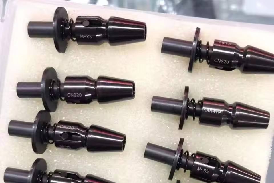
A 5G RF part is not simply a part on a board. It is a tiny electric environment.
A filter, LNA,, RF button, duplexer, coupler, oscillator, antenna module, or mmWave bundle just acts as defined when the PCB stack-up, solder joint geometry, grounding, through transitions, return course, dielectric material, and thermal course behave also. I do not trust any type of RF quote that begins with element cost and ends with distribution day. The actual quote is buried in process capacity.
And process capacity is where many teams obtain subjected.
For RF motherboard setting up, I would rather see an unsightly process home window with real dimension information than a glossy assurance concerning “accuracy.” Accuracy needs to suggest paste quantity control, placement balance out data, reflow profiling, invalidating limits, AOI policies, X-ray standards, resistance promo code results, and last RF examination connection.
NIST’s 2024 work on broadband RF permittivity is a helpful warning. In a study on 3D integrated glass frameworks, researchers defined removing dielectric permittivity from 100 MHz to 30 GHz utilizing S-parameter dimensions, keeping in mind that permittivity and loss tangent impact signal transmission, parasitical capacitance, and crosstalk in microwave-frequency structures relevant to 5G and 6G devices. That is not lab facts. That is why a “exact same Gerber, cheaper laminate” choice can trash a microwave circuit assembly.
The Hidden Manufacturing Variables Behind High-Frequency Circuit Assembly
The most effective RF parts for 5G circuits are not always one of the most expensive parts. They are the components whose electric habits survives the develop.
That indicates they make it through pattern print, pick-and-place shock, nitrogen reflow, board cleaning, assessment, depaneling, coating if used, product packaging, delivery, and area temperature level biking. An exceptional power amplifier on a terribly profiled board is simply a costs warmth resource.
For early design builds, regulated Прототипы и мелкосерийные линии SMT make more sense than making believe a lab run is production. The early concern is not “Can we develop 10 boards?” The far better question is whether those 10 boards expose sufficient variant to forecast what takes place at 1,000, 10,000, or 100,000 systems.
That is where high regularity PCB design becomes political. The RF engineer wants low-loss laminate. Procurement wants a second resource. Manufacturing desires reduced warp, cleaner handling, typical pattern guidelines, and fewer reflow surprises. Quality wants inspection requirements that endure an audit.
Everyone is right. Every person is likewise incomplete.
RF Assembly Control Information That Actually Matter
| Setting up Variable | Why It Matters for RF Components | What I Would Demand Prior To Manufacturing |
|---|---|---|
| Dielectric constant, Dk | Changes impedance, stage, filter response, and antenna adjusting | Managed laminate great deal information, insusceptibility promo codes, stack-up evaluation |
| Dissipation factor, Df | Transforms signal right into warmth and insertion loss | Material certificate plus RF validation, not datasheet approval |
| Copper roughness | Increases conductor loss at high frequency | Specified foil type and surface treatment, especially over a number of GHz |
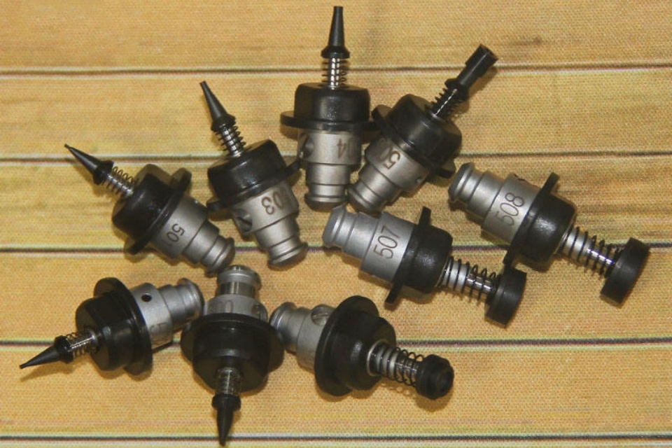
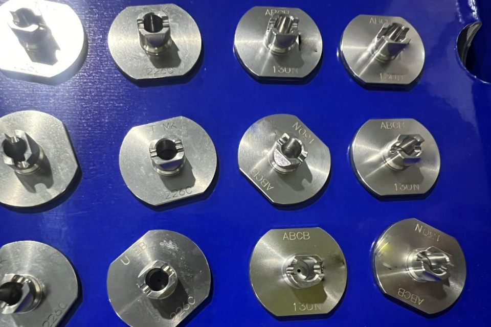
| Stencil aperture style | Modifications solder height, parasitics, and grounding | Paste quantity research for guards, QFNs, LGAs, RF modules |
| Via sewing and basing | Controls return present and shielding actions | DFM review before design release, not after very first failings |
| Профиль для дожигания | Impacts nullifying, warpage, moistening, and component anxiety | Board-level thermal profiling with real component mass |
| AOI and X-ray method | Standard AOI may miss RF-killing flaws | Evaluation restricts linked to electric failure modes |
| Last RF examination | Validates genuine setting up actions | S-parameter, gain, noise number, power, or adjusting tests as required |
And no, “IPC Course 2” is not enough by itself.
That declaration aggravates people, which is why I maintain making it. IPC workmanship regulations assist, however RF actions can fall short inside aesthetically acceptable geometry. A somewhat extreme solder fillet can come to be a parasitical structure. A ground space can elevate inductance. A trace transition can radiate. A shield can look seated and still leak power.
The 2024 IEEE International Roadmap for Instruments and Systems factors in the same direction. Its RF and analog discussion flags pressure around amplifier efficiency at greater operating regularities, small multi-band antennas, and high-efficiency directional antennas. Those are not isolated design issues. They come to be setting up troubles the minute the board strikes the line.
Just How to Assemble High-Frequency RF Circuits Without Guesswork
Begin with the stack-up.
Lock the controlled resistance targets, dielectric material, copper profile, solder mask approach, by means of rules, and RF launch geometry prior to the BOM is “optimized.” Then compel the SMT process to match the electric intent. If you are developing an RF front-end board, 5G small-cell module, antenna control board, phased-array subassembly, or microwave sensor device, the process plan should obtain the same interest as the schematic.
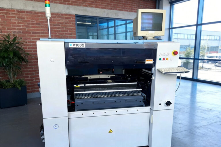
For production, the tools mix matters. A severe Решение для линии SMT под ключ for 5G PCB setting up should not be marketed as a generic conveyor-to-reflow plan. It requires placement repeatability, feeder dependability for little passives, managed print high quality, deducible reflow data, inspection deepness, and solution action when return starts drifting at the worst possible time.
I care a great deal concerning reflow. Greater than several customers intend to hear.
RF assemblies typically integrate 01005 or 0201 passives, guard containers, QFN or LGA RF ICs, filters, ports, and thermal pads on boards that may make use of hybrid materials. Thermal mass mismatch is not a detail. It is where voids, tombstones, cold joints, and unpredictable RF habits are birthed. A great термопрофилировщик для пайки is not a device in this context. It is evidence.
Inspection, Test, and the Expense of Counterfeit Financial Savings
Examination is where the market usually gets lazy.
Requirement AOI captures polarity, missing out on parts, skew, bridges, and apparent solder concerns. Fine. However RF failure commonly conceals under bundles, shields, and ground pads. That is why a properly picked Система контроля SMT should be tied to the well-known failure physics of the assembly, not merely to a common flaw collection.
In high-volume programs, the discussion adjustments once more. Once RF yield is stable, throughput becomes the blade. At that phase, high-speed automation SMT lines make good sense just if the process home window has currently been shown. Rate prior to stability is how makers create costly scrap with self-confidence.
And for customers chasing after lower price, right here is the difficult truth: RF elements do not forgive fake financial savings.
A less costly solder paste, a substituted laminate, a reduced inspection step, an unproven feeder configuration, or a rushed reflow profile can conserve cents while moving failings into last RF examination, field returns, or periodic customer grievances. Recurring RF mistakes are the most awful kind. They squander design weeks and make everybody look guilty.
FAQ: 5G RF Elements and High-Frequency Circuit Setting Up
What are RF elements in 5G circuit assembly? RF components in 5G circuit setting up are parts that create, filter, amplify, switch, path, song, or receive radio-frequency signals throughout sub-6 GHz, C-band, and millimeter-wave systems. They consist of power amplifiers, low-noise amplifiers, filters, duplexers, RF switches, oscillators, couplers, antennas, connectors, and integrated RF front-end modules.
Just how is high-frequency circuit setting up different from conventional SMT assembly? High-frequency circuit setting up is SMT assembly where small physical variants can alter electrical actions at RF and microwave frequencies. Unlike conventional digital or power boards, RF assemblies are sensitive to impedance shifts, dielectric loss, copper roughness, solder geometry, by means of inductance, protecting leakage, port launch top quality, and return-path connection.
What is the best PCB material for 5G RF parts? The best PCB product for 5G RF parts is usually a low-loss laminate with stable dielectric continuous, reduced dissipation aspect, regulated copper roughness, and predictable thermal behavior. Material option depends upon frequency, power, antenna design, board density, expense target, and manufacturing volume.
Just how do you set up high-frequency RF circuits accurately? You assemble high-frequency RF circuits reliably by locking the stack-up early, validating regulated resistance, regulating solder paste quantity, using precise positioning, profiling reflow on the actual board, examining hidden joints, and associating RF test failures with process information. The objective is repeatable electric actions, not simply acceptable solder joints.
Why do 5G PCB settings up stop working after passing aesthetic evaluation? 5G PCB assemblies can stop working after aesthetic examination because RF issues are commonly electric, geometric, or material-based rather than visibly damaged. A board might look appropriate while experiencing excess solder parasitics, weak ground connection, dielectric variant, connector launch inequality, shield leak, or nullifying under thermal pads.
Last Takeaway
RF manufacturing is not magic. It is self-control with receipts.
If you are intending a 5G RF construct, do not start with the maker checklist alone. Start with the failure settings, examination strategy, laminate danger, reflow account, and evaluation evidence. Then develop the line around that truth. For devices preparation or process review, make use of the engineering call channel and bring the stack-up, BOM, target volume, board measurements, RF test demands, and yield pain points.