Three words: stop guessing.
Tombstoning is one of those defects that makes teams fight. Operators blame the pick-and-place. Process engineers blame the reflow. Quality blames “materials.” Meanwhile your real enemy is asymmetry—uneven wetting forces, uneven heating, uneven paste volume, uneven pad design—stacked together until a 0201 decides it would rather stand up than do its job.
And yes, I’m going to be blunt: if your first move is “recalibrate the mounter,” you’re often wasting hours.
Because tombstoning (chip standing) in pick and place is rarely born at placement. It’s usually enabled there and executed in the oven.
So what’s actually happening?
A chip resistor/capacitor has two terminations. During reflow, solder on one end wets first or pulls harder. That end anchors. The other end lags. Surface tension becomes a tiny crane. The component rotates upright. You get an open circuit, a latent reliability headache, or both.
If you ship enough volume, this turns from “annoying defect” into “career-limiting event.” The U.S. regulator record is full of reminders that solder joint defects can become safety issues—like NHTSA recall documentation describing cracked solder joints on a PCB leading to rear visibility problems. That’s not tombstoning, but it’s the same moral lesson: process escapes scale into public problems. (static.nhtsa.gov)
The hard truth about “pick-and-place caused it”
Pick-and-place can contribute. But it’s usually not the root cause.
Here’s the hierarchy I trust when I’m staring at yield charts and arguing with people who want a single villain:
- Stencil printing + pad design create the imbalance
- Thermal gradients + reflow profile amplify the imbalance
- Placement either reduces the risk (good contact, centered, correct Z) or increases it (skew, bounce, poor seating)
That’s why the fastest teams don’t “hunt tombstones.” They instrument the line. They run SPI data. They correlate AOI calls to printer offsets. They treat reflow profile like a controlled experiment, not a folk recipe.
If you don’t already run that way, start with your own process backbone—your internal process quality controls and the boring-but-effective discipline that comes with them.

Tombstoning causes in SMT: the real list (not the polite one)
1) Paste volume imbalance (the printer did it, quietly)
One pad gets more paste. Or paste deposits smear. Or the stencil aperture design feeds one side differently.
Typical offenders:
- Aperture mismatch left vs right pad
- Clogging on fine apertures (Type 3 paste pretending it can do 01005 all day)
- Squeegee pressure/speed drift creating directional volume bias
- Board support issues causing inconsistent gasketing
What it looks like in data:
- SPI shows one pad consistently +15–30% volume vs its mate (same reference designators, same location trend)
- Tombstones cluster in a printer direction (left edge, trailing edge, same board quadrant)
If you want “chip standing defect pick and place” to drop fast, printer discipline is where the money is.
2) Pad design and copper imbalance (your PCB layout set a trap)
Pads aren’t truly symmetric. Copper pours pull heat. Thermal relief differs. Vias sit near one pad. Solder mask definitions differ.
This gets ugly on:
- 0402 → 0201 → 01005 scaling
- boards with heavy copper planes on one side of a chip
- mixed thermal mass neighborhoods (tiny passives parked next to big inductors or connectors)
If you run lead-free SAC305 (Sn96.5/Ag3.0/Cu0.5), the wetting timing is less forgiving than old-school SnPb. That’s not nostalgia. That’s physics and process window.
3) Reflow profile timing (your oven “fixed” one defect by creating another)
Ramp rate, soak time, TAL, peak—everyone has opinions. Most are untested.
Tombstoning increases when one pad reaches wetting conditions earlier than the other. Aggressive ramps and uneven soak behavior can make that worse, especially with miniaturized parts. There’s academic work showing how reflow parameters interact with miniaturization and joint integrity—worth reading if you want fewer arguments and more knobs you can actually control. For example, this 2023 study on reflow profile factors and miniaturisation focuses on solder joint integrity under different profiles. (Springer article) (Springer)
My unpopular take: lots of lines run “fast” profiles because throughput feels tangible, while defect risk feels abstract. Then the rework queue becomes your real bottleneck.
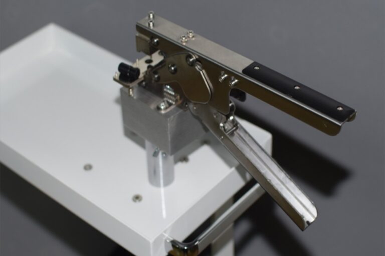
4) Placement mechanics (the mounter didn’t cause the physics, but it can trigger it)
Placement issues that raise tombstoning probability:
- Off-center placement (one termination barely contacts paste)
- Too-high placement height (component “floats,” paste doesn’t tack evenly)
- Excess placement force (paste squeezes asymmetrically)
- Nozzle wear/contamination causing micro-tilt
- High-speed placement on tiny passives with marginal board support
This is where “pick and place” belongs in the story: not as the main suspect, but as the risk multiplier.
If your line is a mix of NPI and volume, tune setups differently. Don’t pretend a prototype line and a mass-production line share the same stable window. If you’re building that kind of flexibility, your reference should be something like prototype & small-batch SMT line setups versus high-speed mass production lines, because the operating assumptions are different.
5) Materials variability (the excuse that sometimes is real)
I’ve seen “same part number” behave differently across lots because termination plating, solderability, and storage history weren’t as consistent as purchasing wanted to believe.
But don’t jump here first. It’s the classic trap: blaming the vendor is emotionally satisfying, and technically lazy.
Tombstoning vs skewing vs bridging (stop mixing these up)
Tombstoning: one end lifts fully. Skewing: the chip rotates but stays down. Bridging: solder connects pads that shouldn’t be connected.
They share parents (print + reflow), but they don’t share the same dominant mechanism. The fix you use for bridging (reduce paste, tighten aperture) can increase tombstoning if it creates a “low paste” pad on one side. That’s why single-metric optimization is how lines get unstable.
A field-ready troubleshooting sequence (fast, not elegant)
Short sentence. Start at SPI.
Now do this like you’re paid for results, not for theories: pull the last 200–500 placements worth of SPI volume/height/area for the tombstoning reference designators, slice by board location, correlate with printer side/offset, then check whether the defect clusters align with a single stencil aperture family or a single thermal neighborhood—because once you see the pattern, you’ll stop blaming the wrong machine.
Rhetorical question: why argue when you can plot it?
Also, if you don’t have in-house confidence on doing that analysis, get training that’s actually tied to defect closure, not sales demos—this is exactly where training and after-sales support pays back.
The numbers that matter (and what they tell you)
Below is a practical “root cause map.” It’s not theoretical. It’s how you sort signal from noise on a running SMT line.
| Suspect | What you see at AOI | What SPI / logs usually show | Quick test | Prevention / fix |
|---|---|---|---|---|
| Paste volume imbalance | Tombstones cluster by board quadrant or print direction | One pad consistently higher volume/height than its mate | Rotate board 180° (if possible) and watch defect pattern shift | Redesign apertures, clean stencil cadence, stabilize squeegee settings, improve board support |
| Pad/copper thermal imbalance | Tombstones near large copper pours or heat-sinks | SPI OK, but defects correlate with “hot/cold” neighborhoods | Add thermocouples on both pads of the same component | Balance copper, adjust thermal relief, revise land pattern, consider mask-defined pads |
| Aggressive ramp / weak soak | Random-looking tombstones, worse on tiny passives | Oven logs show high ramp (e.g., >2–3°C/s) or short soak | Slow ramp and extend soak slightly; compare defect rate | Tune profile: reduce ramp, improve soak uniformity, verify TAL stability |
| Placement offset / poor seating | Tombstones appear with other placement-related calls (skew, insufficient contact) | Placement data shows systematic offset; nozzle maintenance overdue | Reduce speed for passives and recheck Z-height / force | Center placement, maintain nozzles, tune placement height/force, improve board clamping |
| Paste chemistry / solderability | Defect spikes after paste change or material lot change | SPI sometimes normal; wetting timing changes | Swap back to prior lot/paste; run A/B trial | Tighten incoming controls, storage rules, paste life tracking, verify solderability |
One more “hard truth” point: solder joint reliability failures don’t wait politely. A 2024 review paper in Materials notes how dominant solder-joint-related failure mechanisms are in electronics packaging and assemblies, and it puts real weight behind why process escapes matter beyond cosmetics. (MDPI paper) (MDPI)
Prevention methods that survive scale
Make symmetry boring again
- Match apertures left/right for passives unless you prove you need intentional imbalance
- Use SPI limits that compare pad-to-pad, not just absolute volume
- Track paste type by design class (Type 4/5 for ultra-fine; don’t “make it work” with heroics)
Tune reflow like an experiment, not a tradition
- Put thermocouples on both pads for the same chip in a problem zone
- Optimize for wetting synchrony, not just peak temperature
- Validate changes with defect rate + pull strength/shear data when possible
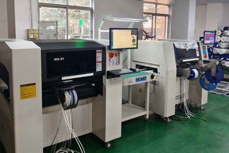
Treat pick-and-place as a precision system, reminder: it drifts
If you’re running Yamaha, Panasonic, JUKI, Hanwha, Fuji—doesn’t matter—the drift patterns look different, but drift exists. Nozzles wear. Feeders age. Z calibration isn’t immortal.
And this is where your vendor’s “we’ll help you” claims get tested. If you care how support actually works, read the service promise with the same skepticism you apply to placement accuracy brochures.
Document the fix so it sticks
The difference between a good line and a chaotic line is whether the fix becomes a standard. If you want fewer repeat defects, show the team the data, and keep the evidence trail in your internal knowledge base.
If you need reference workflows, your own turnkey SMT line solutions documentation should include defect-closure loops, not just equipment lists.
FAQs
What is tombstoning (chip standing) in SMT?
Tombstoning is a reflow-soldering defect where a small passive component (typically a chip resistor or capacitor) lifts and stands upright because solder wets one end earlier or pulls harder, creating an unbalanced surface-tension torque that pivots the part into a vertical position and leaves an open circuit. After that definition, the key point is this: tombstoning is a timing and symmetry problem. Fixes that restore equal wetting on both ends usually win.
Why do chips tombstone during reflow?
Chips tombstone during reflow because the two terminations experience different wetting forces and wetting times, often driven by uneven solder paste volume, uneven pad/copper heating, or a reflow profile that makes one side reach liquidus and wet first, allowing surface tension to rotate the component upright. If you want proof, place thermocouples on both pads of the same chip and compare wetting timing after profile tweaks.
Is tombstoning caused by pick-and-place accuracy or reflow?
Tombstoning is primarily a wetting-imbalance defect created during reflow, while pick-and-place accuracy and placement mechanics mostly influence the probability by changing how well each termination contacts paste and how symmetric the starting condition is when the board enters the oven. So yes, placement matters, but the oven is where the “standing up” happens.
What’s the best reflow profile to reduce tombstoning?
The best reflow profile to reduce tombstoning is the one that synchronizes wetting on both pads by controlling ramp rate, soak uniformity, and time-above-liquidus so neither end of the chip reaches strong wetting conditions significantly earlier than the other end, especially on 0201/01005 parts. In practice, teams often reduce ramp aggressiveness and stabilize soak to shrink pad-to-pad temperature differences.
How do I troubleshoot tombstoning fast on a running line?
The fastest way to troubleshoot tombstoning is to correlate AOI defect calls with SPI pad-to-pad volume/height imbalance and board-location clustering, then run a controlled A/B test that changes only one variable (printer settings, aperture cleaning cadence, or reflow ramp/soak) to see which change breaks the pattern. If you can’t graph it, you’re guessing. If you can graph it, you’re close.
How is tombstoning different from skewing and bridging?
Tombstoning is a vertical lift of one termination caused by unbalanced wetting forces, skewing is a lateral rotation while the component stays down (often from placement offset or uneven paste), and bridging is an electrical short where solder connects adjacent pads because paste volume, pad spacing, or reflow behavior allows solder to merge. Mixing these up wastes time because the “best fix” for one can worsen another.
Conclusion
If you want, send me your component size (0402/0201/01005), solder alloy (SAC305 vs SnPb), paste type (Type 3/4/5), and your current ramp/soak/TAL. I’ll tell you what I’d test first—and what I’d ignore. Start here: contact our team